








Policy Update
Purbaa Jagannath
Background
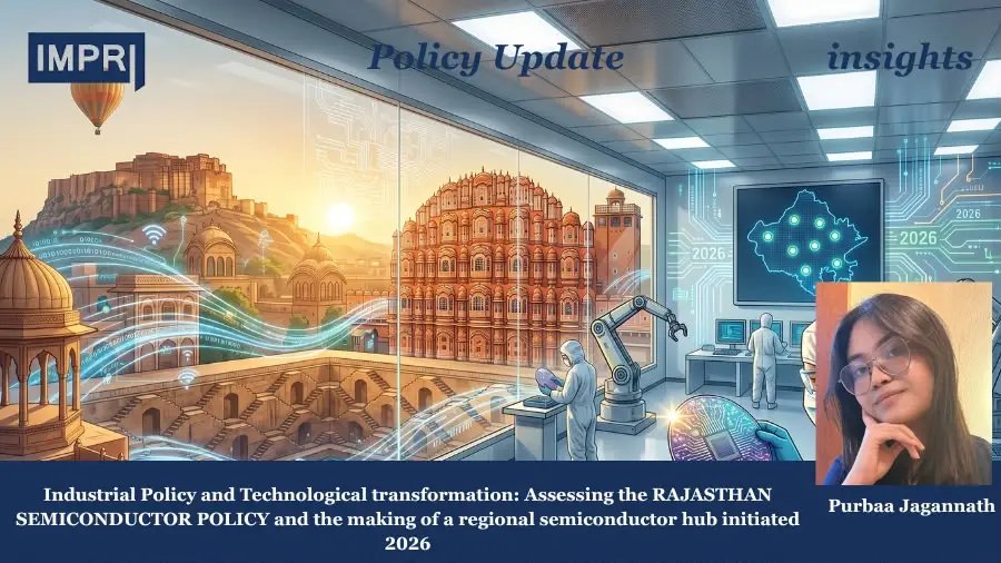
On 18 March 2026, the Government of Rajasthan approved the Rajasthan Semiconductor Policy 2026, formally released as a policy document by the state government on 24 March 2026. The policy was introduced against the backdrop of India’s broader semiconductor push under the India Semiconductor Mission (ISM) and reflects a deliberate attempt by the state to move away from its traditional industrial base of textiles, mining, and handicrafts toward a technology-driven growth model aligned with the state government’s “Viksit Rajasthan-2047” vision.
The rationale for the policy lies in the growing strategic and economic importance of semiconductors, which now underpin electronics, telecommunications, automobiles, defence systems, and the digital economy. With India importing the vast majority of its chip requirements, both the central and state governments have identified semiconductor manufacturing as a priority sector for investment, employment generation, and technological self-reliance.
The policy’s core objectives are to attract large-scale investment into Outsourced Semiconductor Assembly and Test (OSAT), Assembly, Testing, Marking and Packaging (ATMP), sensor manufacturing, and advanced electronics; to build a skilled workforce through dedicated semiconductor academies and design labs; to nurture a fabless chip-design ecosystem; and to position Rajasthan within global semiconductor supply chains. The intended beneficiaries include semiconductor and electronics manufacturers, fabless design startups, engineering graduates and technical workers, and, indirectly, downstream industries such as electric vehicles, defence electronics, and telecommunications equipment.
Key provisions include the development of dedicated semiconductor corridors and clusters, notably in the Jodhpur-Pali-Marwar industrial belt, the Kankani Industrial Area, and the Bhiwadi-Khushkhera belt near the Delhi-NCR region, along with plans for world-class fabricator parks. The policy aligns itself explicitly with national programmes such as Make in India, the Electronic Systems Design and Manufacturing (ESDM) scheme, the Semicon India Programme, and the India Semiconductor Mission.
Functioning
The policy operates through a single-window clearance mechanism designed to fast-track land allotment, statutory approvals, and infrastructure provisioning for semiconductor and electronics investors. Identified industrial corridors are being upgraded with uninterrupted electricity and water supply, improved road connectivity, and dedicated utility infrastructure, with the explicit goal of building an integrated ecosystem rather than a set of disconnected industrial units.
On the funding side, the policy layers state-level incentives on top of central support available through the ISM. Eligible industries receive a grant equivalent to 60 percent of the capital subsidy approved under the India Semiconductor Mission, along with a 5 percent interest subvention on term loans to encourage capital investment. Additional fiscal incentives include exemptions on electricity duty, stamp duty, and land conversion charges. The policy also embeds environmental sustainability into its incentive structure: eligible units receive 50 percent reimbursement of expenditure on environmental protection measures, a full electricity duty exemption for seven years for projects powered by captive renewable energy, and a 50 percent concession on consent fees under the Rajasthan Green Rating System.
In terms of implementation status, the state’s first tangible outcome has been the semiconductor cluster at Salarpur-Khushkhera in Bhiwadi, spread over more than 50 acres, positioned as India’s first dedicated small and medium enterprise semiconductor facility. A separate ATMP/OSAT unit at Bhiwadi, developed under the central government’s Scheme for Promotion of Manufacturing of Electronic Components and Semiconductors (SPECS), was inaugurated on 15 May 2026 and is counted as India’s thirteenth approved semiconductor unit nationally, though it sits outside the main ISM project list.
The principal fiscal incentives under the policy are summarised in Table 1.
| Incentive Category | Policy Details |
| Capital Subsidy | Eligible industries receive a grant equivalent to 60% of the capital subsidy approved under the India Semiconductor Mission (ISM). |
| Interest Subvention | The state offers a 5% interest subvention on term loans to encourage capital investment. |
| General Exemptions | The policy provides exemptions on electricity duty, stamp duty, and land conversion charges. |
| Environmental Subsidy | Eligible units receive a 50% reimbursement on expenditures related to environmental protection measures. |
| Green Energy Benefit | Projects powered by captive renewable energy receive a full electricity duty exemption for seven years. |
| Green Rating Concession | Investors are granted a 50% concession on consent fees under the Rajasthan Green Rating System. |
Provisions of the Rajasthan Semiconductor Policy 2026
Performance
Since the policy is barely five months old, performance can only be assessed through early implementation indicators rather than multi-year trend data. At the Bhiwadi cluster, twenty companies have reportedly committed investments exceeding 1,200 crore rupees, of which eleven firms are already operational, generating close to 2,700 jobs in the region. More than half of the cluster’s output is reported to be export-bound, with shipments to markets including Germany and Nepal, suggesting early integration into global value chains rather than purely import-substitution manufacturing.
At the national level, the policy’s performance must be read alongside the trajectory of the India Semiconductor Mission itself. As of mid-2026, thirteen semiconductor projects had been approved across seven states under ISM and SPECS, with cumulative committed investment exceeding 1.6 lakh crore rupees.
The Union Cabinet’s approval of India Semiconductor Mission 2.0, with a fiscal outlay in the range of 1.25 to 1.27 lakh crore rupees and an extended twelve-year programme lifecycle, considerably strengthens the funding pipeline that Rajasthan’s state-level incentives are designed to supplement. Officials have framed the state’s competitive positioning around a “Triple-S” advantage, referring to the availability of silica-based raw materials, a technically skilled workforce, and abundant solar energy potential for powering energy-intensive fabrication and packaging operations.
Impact
It is too early to evaluate whether the policy has met its stated objectives of large-scale investment, employment generation, and technological self-reliance, since most of its provisions remain in early implementation. However, initial indicators point toward measurable, if modest, traction: the Bhiwadi cluster’s operational units and job numbers represent tangible outcomes rather than announcements alone, and the export orientation of early production suggests the emergence of genuine manufacturing capability rather than assembly for the domestic market only.
At the same time, the scale of impact achieved so far remains small relative to the scale of ambition set out in the policy and in Rajasthan’s wider industrial vision. The state’s flagship outcome to date is concentrated in ATMP/OSAT and SME-level packaging activity rather than in front-end wafer fabrication, which continues to be dominated by projects in Gujarat, Uttar Pradesh, and other states under the ISM. Whether Rajasthan can move up the semiconductor value chain toward design and fabrication, rather than remaining primarily an assembly and testing location, will be a more meaningful test of the policy’s long-term impact.
Emerging Issues
Several structural challenges are likely to shape the policy’s trajectory going forward. First, semiconductor fabrication and packaging are highly water-intensive processes, and Rajasthan is among India’s most water-stressed states, with large parts of the state, including the Thar Desert region, facing chronic groundwater depletion and rainfall variability. Locating water-intensive industrial clusters in such a context raises questions about long-term resource sustainability that the policy’s environmental incentives do not fully address.
Second, while the policy speaks of building a skilled workforce through semiconductor academies and design labs, translating this ambition into a sufficiently large pool of VLSI designers, process engineers, and cleanroom technicians will take sustained investment in technical education and industry-academia linkages, an area where implementation details remain limited.
Third, Rajasthan’s semiconductor push is being built in a crowded national landscape, with more established and better-resourced clusters emerging in Gujarat’s Dholera and other ISM-anchored states. Sustaining investor interest will require the state to differentiate itself beyond fiscal incentives, which can be replicated by competing states.
Fourth, the coexistence of multiple designated corridors, Jodhpur-Pali-Marwar, Kankani, and Bhiwadi-Khushkhera, raises coordination questions around how infrastructure investment, utility augmentation, and promotional efforts will be sequenced and prioritised across geographically dispersed locations rather than concentrated in a single anchor cluster.
Finally, since a significant share of the incentive structure is pegged to central ISM subsidies, any delay or recalibration in the disbursement of India Semiconductor Mission 2.0 funds could directly affect the pace of investment realisation at the state level.
Way Forward
To convert early momentum into a durable regional semiconductor hub, several measures merit consideration. Water governance should be integrated explicitly into industrial planning for semiconductor corridors, including mandatory water-recycling norms, treated wastewater use, and transparent monitoring of groundwater impact in and around industrial clusters. Skill development commitments should be backed by measurable targets and public reporting on academy enrolment, curriculum design in partnership with industry, and placement outcomes, rather than remaining a general policy aspiration.
Rajasthan would also benefit from a phased approach that consolidates initial infrastructure investment in one or two anchor corridors before expanding to additional locations, ensuring utility reliability and ease of doing business are demonstrably achieved before scaling geographically. Deepening linkages with the fabless design ecosystem, including startup incubation, intellectual property support, and access to design tools, could help the state move beyond assembly and testing toward higher value-addition activities over time. Finally, continuous monitoring and public disclosure of investment realisation, employment generation, and export performance at the Bhiwadi cluster and future sites would strengthen transparency and allow for evidence-based mid-course corrections as the policy matures.
References
Government of Rajasthan. (2026). Rajasthan Semiconductor Policy 2026. Department of Industries, Government of Rajasthan.
India Semiconductor Mission. (2026). Home. Ministry of Electronics and Information Technology. https://ism.gov.in/
IANS. (2026, March 24). Rajasthan govt unveils Semiconductor Policy document to boost investment and create jobs. Newsgram. https://www.newsgram.com/india/2026/03/24/rajasthan-govt-unveils-semiconductor-policy-document-to-boost-investment-and-create-jobs
Indian Infrastructure. (2026, March 25). Rajasthan government unveils semiconductor policy. https://indianinfrastructure.com/2026/03/25/rajasthan-government-unveils-semiconductor-policy/
India Briefing. (2026, May 18). Outside the ISM: How Rajasthan’s Bhiwadi commissioned India’s 13th semiconductor unit. https://www.india-briefing.com/news/rajasthan-semiconductor-india-chip-facility-bhiwadi-specs-44975.html/
The Hans India. (2026, May 19). Rajasthan eyes global semiconductor leadership as state launches first chip manufacturing cluster in Bhiwadi. https://www.thehansindia.com/news/national/rajasthan-eyes-global-semiconductor-leadership-as-state-launches-first-chip-manufacturing-cluster-in-bhiwadi-1077327
BISinfotech. (2026, May 25). Rajasthan emerges as semiconductor manufacturing hub. https://www.bisinfotech.com/centre-rajasthan-govt-push-electronics-semiconductor-investments/
Republic World. (2026, July 15). Union Cabinet approves India Semiconductor Mission 2.0 with mega outlay of Rs 1.25 lakh crore. https://www.republicworld.com/business/union-cabinet-clears-india-semiconductor-mission-ism-2-point-0-outlay-extended-timeline-2026-07-15-132375
The Hans India, “Rajasthan eyes global semiconductor leadership as state launches first chip manufacturing cluster in Bhiwadi” — https://www.thehansindia.com/news/national/rajasthan-eyes-global-semiconductor-leadership-as-state-launches-first-chip-manufacturing-cluster-in-bhiwadi-1077327
Republic World, “Union Cabinet Approves India Semiconductor Mission 2.0 With Mega Outlay Of Rs 1.25 Lakh Crore” — https://www.republicworld.com/business/union-cabinet-clears-india-semiconductor-mission-ism-2-point-0-outlay-extended-timeline-2026-07-15-132375
The Pioneer, “Finance Ministry panel clears Rs 1.25 lakh cr outlay for ISM 2.0” — https://dailypioneer.com/news/finance-ministry-panel-clears-rs-1-25-lakh-cr-outlay-for-ism-2-0
About the Contributor
Purbaa Jagannath is an intern with IMPRI, contributing to the Policy Update series. Her research interests lie in gender and development policy, women’s economic empowerment, and the care economy in India. She is currently pursuing her Master’s in Social Work at the Tata Institute of Social Sciences, Mumbai.
Acknowledgements
The author extends sincere gratitude to the IMPRI team for their guidance and support, along with the reviewers Shruti Sethi and Lubina Dua for reviewing and adding suggestions
Read More at IMPRI:
Bihar’s Fertility Rate and the Governance Gap: What Policy Is Missing
The Malabar Salinity Frontier: Policy Blind Spots in Non-Kuttanad Estuarine Agriculture